We've updated publication list on our website, and reached a milestone! Feel curious to dive into more than 50 publications investigating Gallium Nitride power devices!

![]()
![]()
![]()
![]()
The different goals set in the InRel-NPower project have been divided in several packages. The projects' technical work packages follow a bottom-up cascade methodology, where every work package provide material for the subsequent packages, and in return receives valuable feedback on the developed structures.
WP lead: J. Derluyn, EpiGaN (Contact)
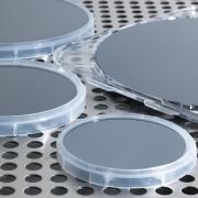 Work package 1 covers the epitaxial techniques and the study of the Ga- and Al-nitride materials that form the basis of the device development in WP2 (Device Processing) and in support of all other work packages.
On the one hand, based on existing background knowledge and projects, we will continue to study GaN-on-Si epitaxy, material and devices, mainly focusing on the relationship between epitaxial recipes and layer stacks versus device reliability.
On the other hand, we will investigate the epitaxy, material quality and device layer stacks of AlGaN-based hetero-structures grown on high quality AlN template and bulk material. This will allow us to reduce the overall defect density (as compared to GaN-on-Si) but also to study the benefits of the AlN material properties (e.g. critical electric field and thermal conductivity).
The work will be closely supported by advanced material characterisation in an effort to correlate structural crystal features with properties at the device level (electrical performance such as reliability).
The partners that are active in this work package are EpiGaN, MIE university, Kyushu university, ONSemiconductor, Fraunhofer IISB and Ghent university.
WP lead: F. Medjdoub, CNRF (Contact)
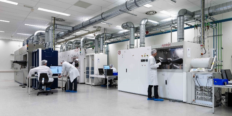
 Work package 2 aims to develop, process and characterize the GaN power devices, for further use in WP3 advanced characterization and in-depth reliability characterization and WP4 assembly and building of the demonstrators. Devices will be processed on GaN-on-Si and GaN-on-AlN substrates developed in WP1. Special focus will be on performance (low on-resistance, high band-gap potential), reliability under stress, robustness and repeatability for large number of samples.
To improve device reliability special focus is on the reduction of vertical and lateral device leakage currents, through optimization of the epi buffer stack (WP1) and the layout of the device through field engineering. The test-chips will also contain the necessary test structures for the optimization of the Ohmic contact. It is believed that (local) removal of the Si substrate under the drain contact will substantially reduce the vertical leakage current, and thus will have a positive impact on reliability. Likewise, replacing the Si substrate by AlN (wide bandgap material) will both improve leakage current and thermal conductivity.
The partners that are involved in this work package are CNRS, ON Semiconductor and Ghent University
WP lead : A. Banerjee, ON Semiconductor Belgium (Contact)
The objective of work package 3 is to identify specific limitations in terms of parasitic effects and reliability issues for GaN lateral power devices. Focus is on the identification of physical mechanisms behind parasitic effects, breakdown effects, long-term degradation phenomena, with the aim of deriving related physical laws and effective qualification procedures. Device safe-operating-area will be determined by the characterization of device breakdown and limitation and extensive reliability evaluation. WP3 will provide feedback to the device and substrate R&D activity of WP1 & WP2 in order to develop a reliable, robust and parasitic free GaN HEMT power technology. Via lifetime predictions, information will be provided to WP4 enabling useable mission profiles for the targeted applications.
More specifically, WP3 will work on :
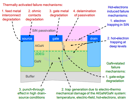
Potential degradation processes affecting lateral HEMT transistors (after M. Meneghini, et al. IEEE Trans. Electron Devices, vol. 62, no. 8, p. 2549, 2015.).
The partners that are involved in this work package are CNRS, ON Semiconductor and Ghent University
WP lead: J. Naundorf, Siemens (Contact)
The main objective of this last technical work package will be the development of two innovative packaging systems and two demonstrators in order to fully exploit the potential of the GaN devices. In summary, the objectives of WP4 are listed here:
This project has received funding from the European Union’s Horizon 2020 research and innovation programme under grant agreement No 720527.