We've updated publication list on our website, and reached a milestone! Feel curious to dive into more than 50 publications investigating Gallium Nitride power devices!

![]()
![]()
![]()
![]()
Our goal is to identify specific limitations in terms of parasitic effects and reliability issues for GaN lateral power devices. Focus is on the identification of degradation mechanisms and prediction of physical models/laws , which can be used for accurate lifetime extrapolation and qualification for GaN based power devices.
From the lab:
News from 2020:
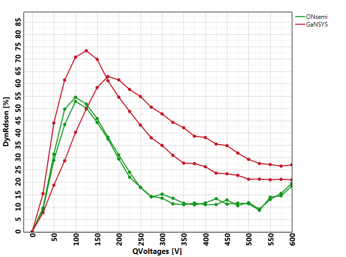
ON Semiconductor’s latest eGaN material showed 2x improvement in Dyn RDS,on as compared to our previous generation devices and also that of GaNSystems (similar gate architecture) as shown in the figure below. All measurements were conducted on packaged level devices (powerbars) using the same conditions (ON: 10usec; OFF: 212 usec) on our Double pulsed tester setup (Auriga).
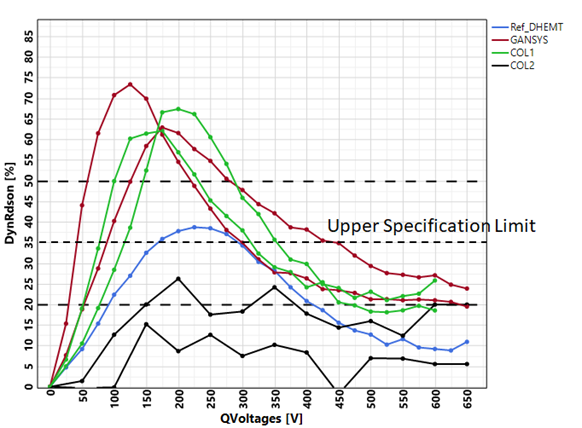
Top figure: showing the comparison between our depletion mode baseline devices, our current “Best” eGaN devices and an equivalent commercially available eGaN device. Measurements were carried out on a double pusled tester for ON state: ~10 uSec; OFF state: ~212 usec.
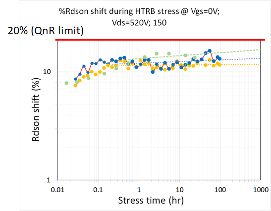
Improvement of HTRB related Degradation Several epitaxial and process related improvements led to solving of the HTRB (VD=520V, VS=VG=Vsub=0V, 150C) related degradation problem. Post 4 day stress, the RDS,on shift was less than 20%, which is the specification limit our technology. The figure below shows the RDS, on degradation of a typical wafer after 4 day stressing.
News from 2019:
|
Achievement of lower Dynamic ON-Resistance as compared to Competitors
Dynamic On-resistance (or current collapse) is one of the major reliability concerns for GaN based power devices. Such phenomenon temporarily increases the On-resistance of the device due to trapping (commonly known as the “Virtual Gate” phenomena) in the gate-drain access region of the device due to off-state stress, which might generate thermal issues leading to device failure. Dynamic RDS,on measurements on our double pulsed tester (Auriga Model AU1580) for faster pulses (ON state: ~10 uSec; OFF state: ~212 usec) were done on our “best” available eGaN split and compared with our depletion mode baseline wafers and a commercially available p-GaN based enhancement mode device. ON semiconductor’s “best” eGaN split exhibited ~55% peak Dynamic RDS,on as compared to the commercially available part (based on similar gate architecture) exhibiting upto 70% of the RDS,on increase as shown in the figure below. Top figure: Dynamic RDS,on measurement comparing ON Semiconductor’s “best” pGaN devices with commercially available devices with similar gate architecture. Data measured on 100 mOhm power transistors. |
|
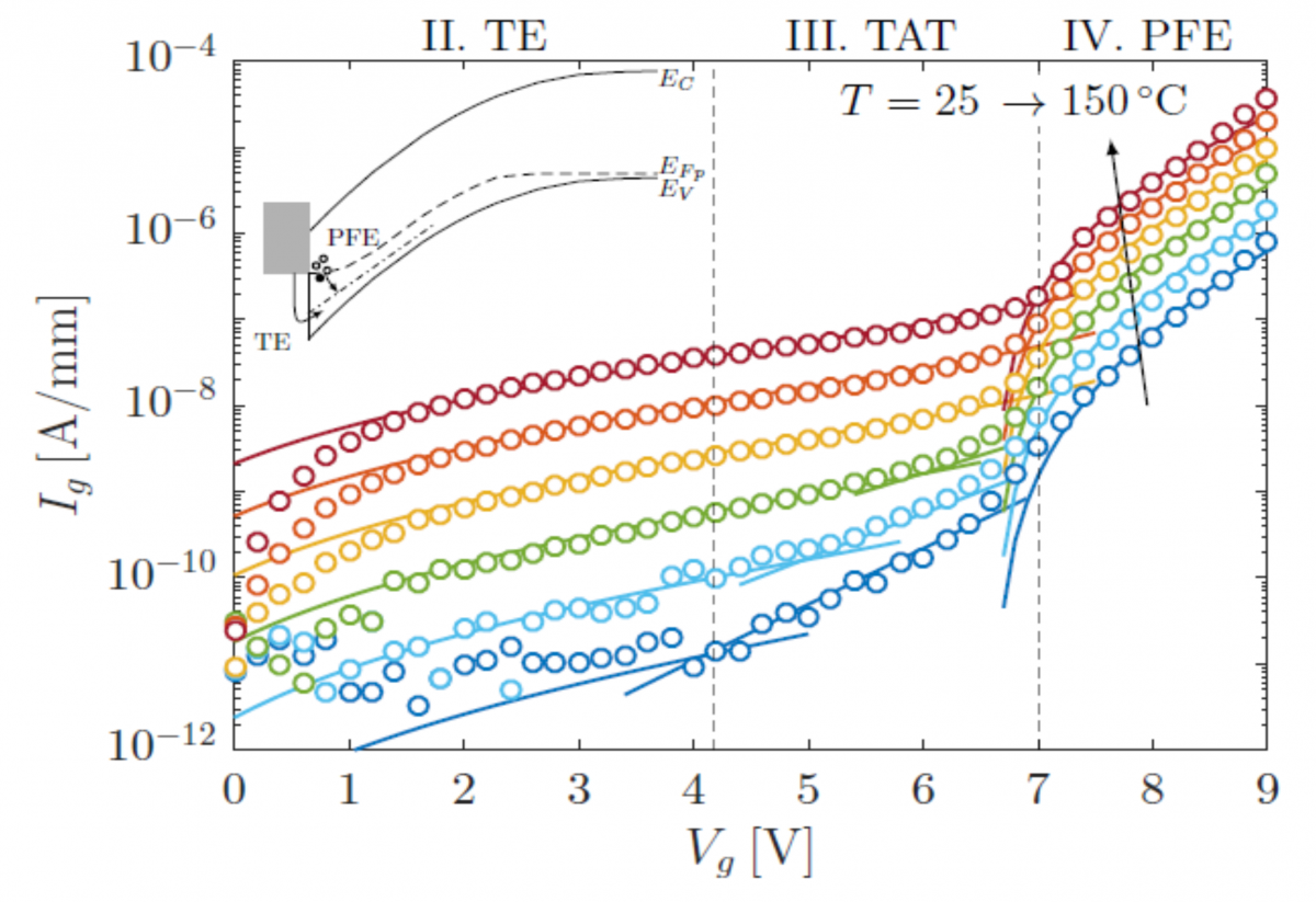
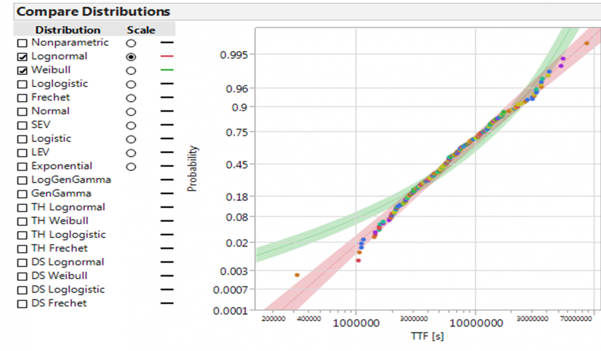
Current conduction through the pGaN gate stack. Symbols : measured data. Full lines : model. The different conduction models in the Schottky diode are indicated. Since the gate structure consists of two back-to-back diodes, the current conduction and the field distribution across the two diodes is not straightforward. Under sufficient forward gate bias, the p-i-n diode is forward biased, and the Schottky is reverse biased. Hence the latter will determine the gate reliability. The figure above shows the Ig-Vg characteristics of the pGaN gate structure, for different temperatures. For Vgs between 4 and 7V, the current conduction is determined by trap assisted tunneling. Above Vgs=7V, Poole Frenkel emission is the dominant mechanism. The information about the current conduction in the Schottky diode is used to extrapolated the TDDB time-to-fail to Vgs=7.25V, T=150oC, see the figure below. All time-to-fail data (obtained from stress tests 7.75V<Vgs<9.25V, and temperatures between 25C and 150oC), fall on one single distribution, which is LogNormal distributed (rather than Weibull). At Vgs=7.25V, T=150oC, for a 100mΩ device size, the expected lifetime at 100ppm is ~105s. Since the device has a Vgs_max=5V, this is well within specification.
TDDB time-to-fail data from stress experiments at different temperatures and gate voltages, extrapolated to Vgs=7.25V, T=150oC, and fitted with a LogNormal (red) and Weibull (green) distribution function. |
News from 2018:
|
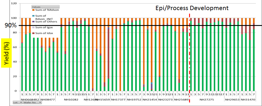
Improvement of yield results in higher production efficiency and reduction in manufacturing costs. High and uniform Yield also indicates a stable and reliable process flow. Over the last 9 months significant focus was devoted to improve the epitaxy/process yield and establishment of a baseline procedure. Since ON Semiconductor’s 650V Depletion Mode GaN Power Transistors were closest to maturity, establishment of the baseline procedure was started on the d-HEMT platform. Yield is calculated based on the unit probe data measured on 140 mm multi-finger power transistors. The measured data is binned as per the specification limit implied on the technology. In case, the device parameter exceeds the specification limits, it is considered as a ‘FAIL’. A few of the major parameters which are currently used for measured data comparison and binning are the Dynamic On-resistance (measured over the whole voltage range upto 650V) and off-state leakages. The current limits used for Dynamic On-resistance and off-state leakages (gate and drain) are 5% (ON: 400us ; OFF: 40 msec) for any quiescent voltage upto 650V and 100nA (absolute value), respectively.
Figure 1, shows a typical graph showing the evolution of Yield over the previous 9 months. As can be observed during the earlier months one of the major reasons for Yield loss was high Dynamic On-resistance followed by high off-state drain leakage. Such “Soft” failures resulted in very fluctuating Yields ranging between ~10% to >90%. Several iterations of epitaxial and device architecture improvement was carried out, which lead to the achievement of an average (and stable) Yield figure of >90%. Dynamic On-resistance issue was significantly reduced. Work in ongoing for even further improvement to reach almost 100% Yield, which is in currently in-line with ON Semiconductor’s future quality roadmap of “Road to Zero Defects”.
Figure 1: Yield graph showing the evolution of Yield figures on ON Semiconductor’s 650V d-HEMT Technology during the previous 9 months. The Yield table consists of several Lots (and including wafers) and is based on unit probe measurement data on 140 mm multi-finger power transistors (>1600 power transistors/wafer). Several iterations of Epi and process development lead to the achievement of an average Yield figure > 90%.
|
|
ON Semiconductor is currently working on the development of a true Enhancement Mode (eGaN) technology based on p-type doped GaN gate architecture. Primary challenges involved in such technological development include development of a low damage and highly selective (pGaN to AlGaN barrier) p-GaN etch recipe in the access regions, achievement of positive threshold voltage, proper passivation of the access regions for suppression of off-state leakages and reduction of Dynamic On-resistance, etc. High etch selectivity of pGaN etch is typically obtained with high Al-content in the barrier, which however, tends to shift the threshold voltage more negative due to the presence of higher number of carriers in the channel because of higher polarization effects. Reduction of Al-content (/%) shifts the threshold voltage positive but reduces the etch selectivity, which leads to higher On-resistance in the access regions. Furthermore, the etch process needs to be fine-tuned in order to eliminate any plasma induced damages (PID) on the etched surfaces (pGaN sidewalls and access regions), which might result in higher Dynamic On-resistance and/or other reliability issues. |
|
|
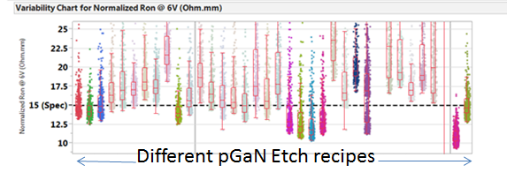
Figure 2a: Figure showing the magnitude and distribution of On-resistance as a function of pGaN etch recipes (denoted by different color codes). The On-resistance is measured on power transistors by forcing 1A on the drain and measuring the voltage drop on the drain for an On-state gate voltage of 6V. |
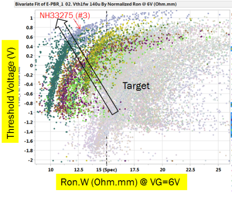
Figure 2b: Figure showing our global threshold voltage versus On-resistance graph for difference etch process splits. Current target is to achieve low On-resistance (<15 Ohm.mm) with threshold voltages of >1.5V. |
|
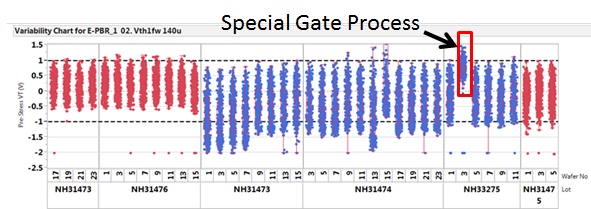
Several etch processes with different etch chemistries, bias power, temperature, pressure etc were tested on similar epitaxial layers for comparison purposes. As can be seen in Figure 2a, both the magnitude and the distribution of the On-resistance can be significantly influenced by the choice of the etch processes and parameters and only a few of such recipes helped us to achieve our 15 Ohm.mm On-resistance target. Figure 2b, shows our global threshold voltage versus On-resistance graph. Such a graph is obtained when the On-resistance data of Figure 2a is plotted against their corresponding threshold voltage values. As can be seen, wafers which meet our On-resistance specifications does not meet the threshold voltage requirements of >1.5V, and are mostly depletion mode devices (negative threshold voltage). One particular wafer, denoted as NH33275 (#3) received a special processing step post pGaN gate etch, which managed to shift the threshold voltage to positive magnitude. A data comparison of threshold voltages comparing different gate processes is shown in Figure 3, proving the fact that not only the barrier’s Al% but also gate module process conditions can have a major impact on the threshold voltage.
Figure 3: Figure showing the data comparing the threshold voltages among the different gate module processing. The threshold voltage is measured at 1uA/mm for VD=1V on power transistors. Almost all the wafers are depletion mode (negative threshold voltage) except NH33275 #3 which showed a positive threshold voltage of ~0.5-1.5V with an on-wafer distribution of ~1V. |
|
This project has received funding from the European Union’s Horizon 2020 research and innovation programme under grant agreement No 720527.